A. Paukštys, founder and president of the Teltonika group of companies, about the latest project in Vilnius: It has been a couple of decades since anyone in Europe has built a new PCB factory
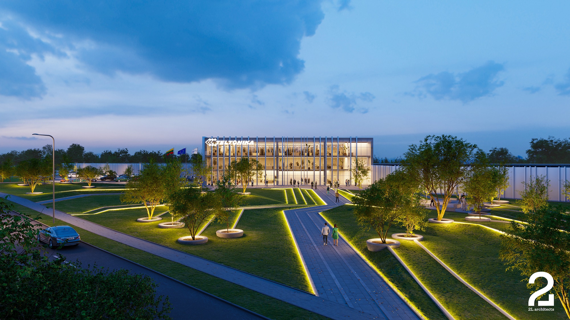
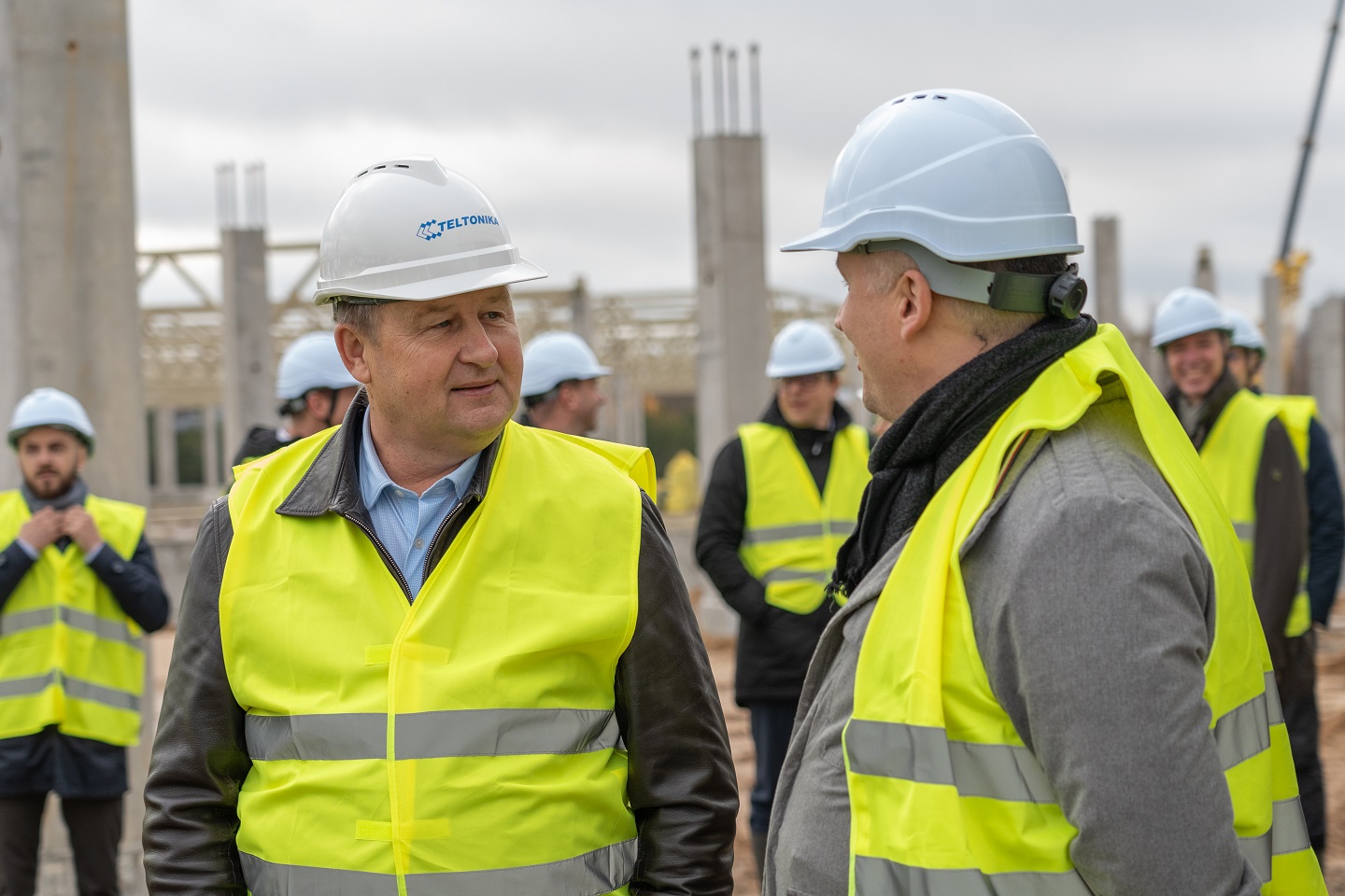
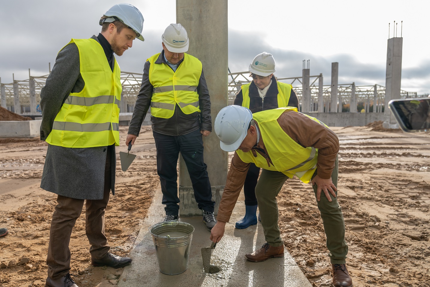
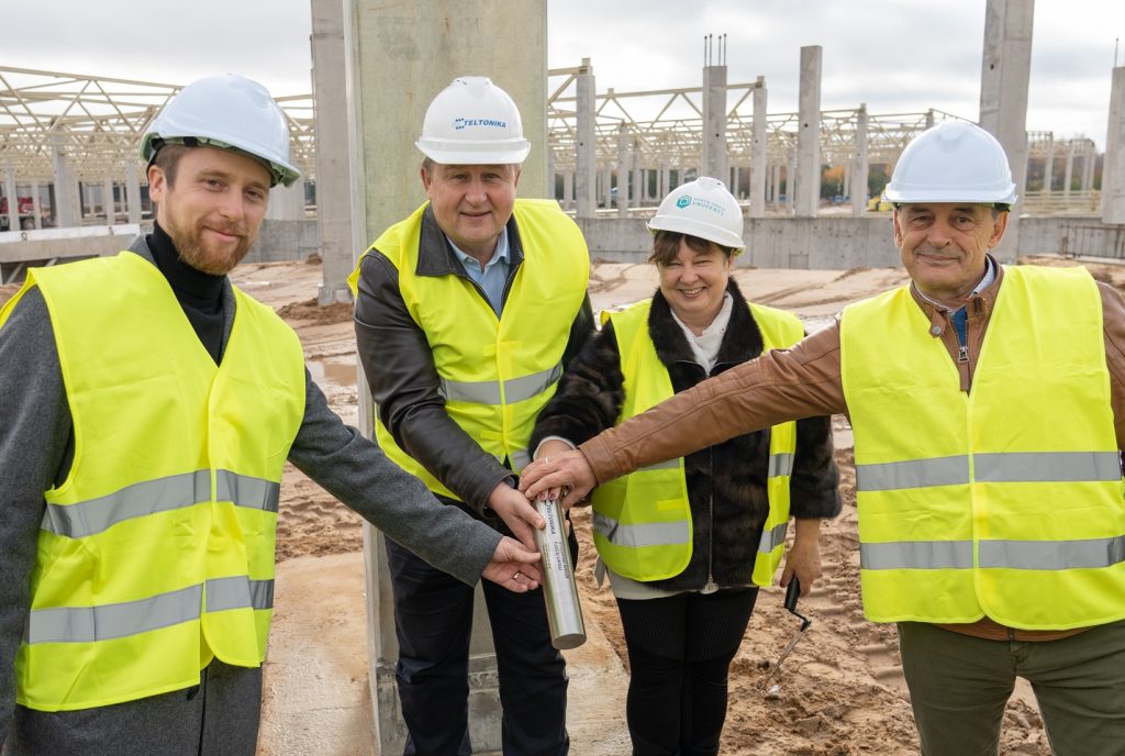
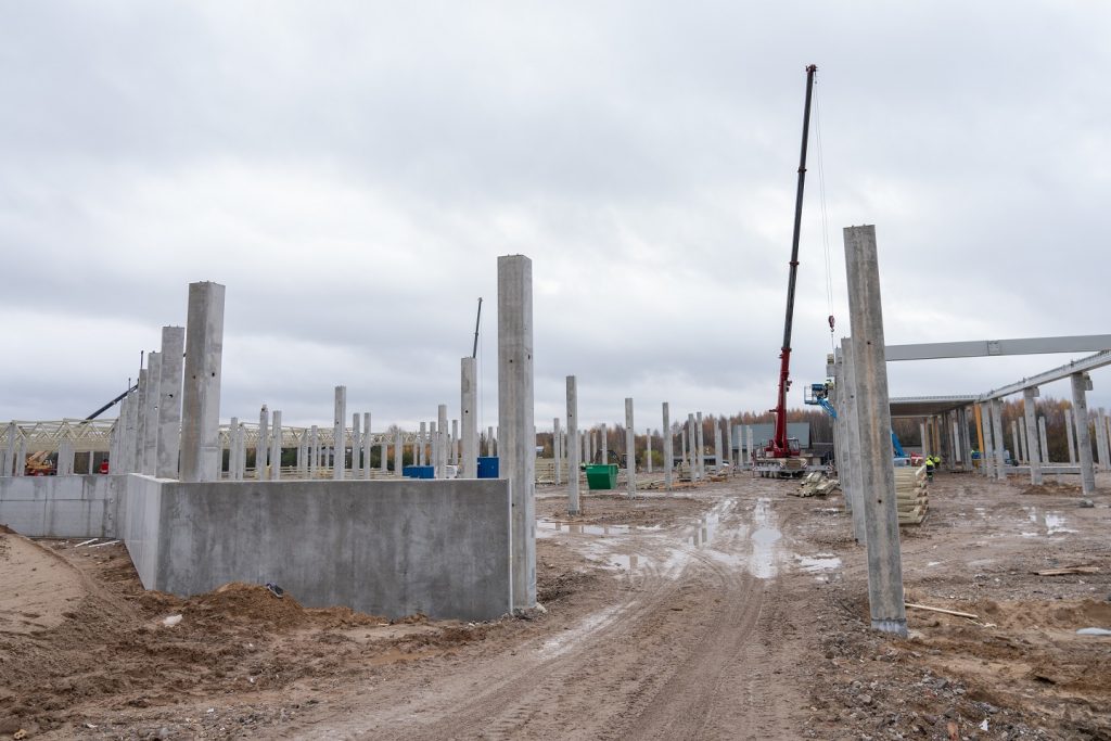
Construction work on the site of the Teltonika printed circuit board (PCB) factory in Vilnius is moving forward rapidly. With the installation of reinforced concrete structures, the outline of the future plant has become clear, and on Tuesday, a symbolic time capsule with a letter to future generations was buried in the foundations of the building.
The 33,000 square metre factory will have the highest level of automation currently available and will employ around 250 highly skilled workers in the factory and administrative areas. The plant is expected to have its roof on later this year, followed by interior fitting-out work. The plant is expected to start operations in early 2025. It will be one of the most advanced plants of its kind in Europe and a unique project on the continent.
“It has been a couple of decades since anyone in Europe has built a new PCB factory. This market is dominated by Asian countries and Europe has a shrinking number of producers. Given these trends, the construction of this plant is of great importance for the further development of the Teltonika company group. This investment will allow us to shorten production lead times, expand intellectual property protection for the technologies we develop, reduce supply chain risks and become independent from third-party political decisions,” says Arvydas Paukštys, Founder and President of Teltonika company group.
A printed circuit board is the base of modern electronic devices on which various components, including semiconductor chips, are placed. Nowadays, this element is hardly replaceable in the manufacturing of more complex electronics.
Teltonika is building a printed circuit board factory as part of a major project investment agreement signed with the Ministry of Economy and Innovation. The investment in the modern plant will amount to €143 million, most of which will be spent on the acquisition of special production equipment. Installation of the equipment is scheduled to start in the middle of next year.
Production processes will be fully digitalised to ensure short lead times and optimum production costs. The plant will specialise in the production of PCBs for high-tech products. It will develop technologies for HDI, SBU, and Flex-Rigid, as well as for the design of high-frequency PCBs.
Some of the mass production technology solutions will be used for the first time in Europe. For example, it will be the first plant on the continent to use only digital solder mask printing technology and Vertical Continuous Plating (VCP) for mass production. There will also be a strong focus on ecology, with wastewater and process water from production being treated and recycled back into production, thus minimising and treating the wastewater generated.
Teltonika is supported in this ambitious project by Rico Schluter, who has extensive experience in this market. He has been working in the PCB industry for more than 4 decades and has helped customers build several such plants during his career.
“After working 41 years in the PCB-industry, personally, I am very proud to be a part of this unique project that will give a significant boost to the European PCB industry and its supply chain. Cooperation with the Teltonika project team is an absolute pleasure and I am very happy that I can share my very long experience in the PCB industry with my Lithuanian project – team members,” says Mr Schluter.
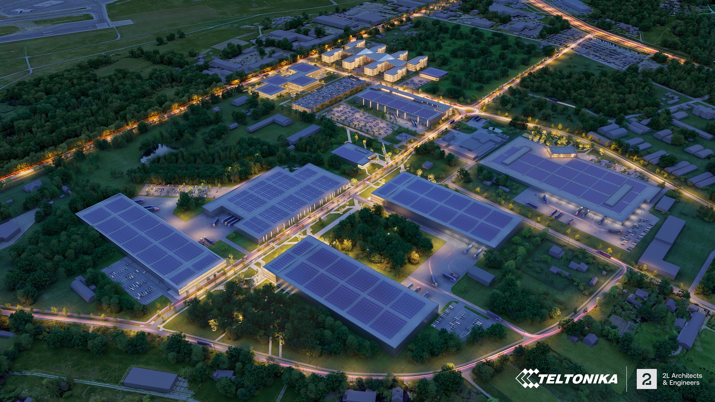
The PCB plant is one of the projects of the Teltonika High-Tech Hill Technology Park being developed in Liepkalnis, Vilnius. Ten new industrial and administrative buildings will be built in several phases over five years, and around 6,000 employees are expected to be employed.
In addition to the PCB factory, new electronic assembly and plastic injection moulding plants, a data centre, offices, laboratories and a commercial building will be built on the 50 hectares of Teltonika High-Tech Hill. A semiconductor chip assembly, testing and manufacturing complex will be a key part of this technology park. The total investment in the Teltonika High-Tech Hill Technology Park over the next decade will be around €3.7 billion.
